
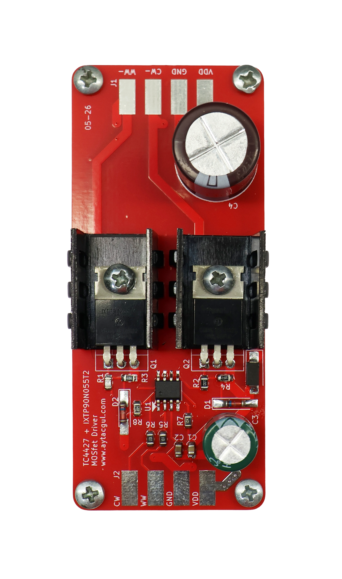
This project is a compact dual-channel MOSFET driver board designed for high-current LED applications where a microcontroller or PWM controller cannot drive the power MOSFET gates efficiently by itself.
I originally designed the board for controlling two independent LED channels, typically CW (Cool White) and WW (Warm White). Each channel uses a dedicated high-current N-channel MOSFET driven by a TC4427A dual MOSFET gate driver.
The board accepts two logic/PWM inputs and switches the corresponding LED channels on the low side. This makes it suitable for high-power LED strips, COB LEDs, lighting experiments, PWM dimming systems and microcontroller-controlled lighting projects.
Why Use a MOSFET Gate Driver?
A power MOSFET gate behaves mainly like a capacitive load. Although practically no DC current is required to keep a MOSFET switched on, a relatively large instantaneous current may be required to charge and discharge the gate quickly.
Driving a large MOSFET directly from an Arduino, ESP32, STM32 or another microcontroller can therefore result in relatively slow switching. During the transition between fully off and fully on, the MOSFET operates in its linear region and dissipates considerably more power.
For low-frequency switching this may not always be noticeable, but it becomes increasingly important when PWM frequency and load current increase.
The TC4427A solves this problem by acting as a high-current buffer between the control signal and the MOSFET gate. It is a dual high-speed MOSFET driver capable of approximately 1.5 A peak gate-drive current per channel.
The device can operate from approximately 4.5 V to 18 V, which also makes a 12 V gate-drive supply very convenient for this circuit.
Hardware Overview
The circuit consists of two almost identical power channels controlled by a single TC4427A.
| Component | Function |
|---|---|
| TC4427A | Dual high-speed MOSFET gate driver |
| 2 × IXTP90N055T2 | Power N-channel MOSFETs |
| 2 × 10 Ω | MOSFET gate resistors |
| 2 × 100 kΩ | MOSFET gate pull-down resistors |
| 2 × 100 Ω | PWM/input series resistors |
| 2 × 100 kΩ | Input pull-down resistors |
| 2 × 12 V Zener | Gate-source voltage protection |
| SMAJ18A | Transient voltage protection |
| 100 nF + 1 µF | TC4427A supply decoupling |
| 1000 µF / 25 V | Bulk supply filtering |
| 2200 µF / 25 V | Load-side bulk filtering |
IXTP90N055T2 Power MOSFET
The output stage uses two IXTP90N055T2 N-channel power MOSFETs in TO-220 packages.
The IXTP90N055T2 belongs to a family of high-current, low-voltage power MOSFETs intended for applications such as switching converters, motor control and other high-current switching circuits.
The device has a nominal drain-source voltage rating of 55 V and a current rating substantially higher than normally required by an LED lighting application. In practice, the usable current of the complete driver is determined not only by the MOSFET specification but also by PCB copper, connectors, heatsinking, ambient temperature and switching conditions.
For this reason I mounted both MOSFETs to relatively large heatsinks. The heatsinks provide useful thermal mass and allow the circuit to operate with considerably larger LED loads than would be practical with an uncooled TO-220 device.
TC4427A Gate Driver
The TC4427A contains two independent non-inverting MOSFET drivers. This makes it particularly convenient for this board because the Cool White and Warm White channels can both be controlled using a single 8-pin IC.
A PWM signal applied to one input produces a corresponding high-current gate-drive signal on the associated output.
The board operates the driver from 12 V. This provides substantially stronger gate drive than directly driving the MOSFET from a 3.3 V or 5 V GPIO.
Using a proper gate driver also reduces the time spent in the MOSFET's transition region. Faster switching generally means lower switching losses, particularly when relatively high PWM frequencies are used.
Gate Resistors
Each TC4427A output connects to its MOSFET gate through a 10 Ω resistor.
Although it might appear preferable to connect the driver directly to the MOSFET gate, a small series resistance is useful. It limits the instantaneous gate current, damps ringing caused by PCB and MOSFET parasitic inductance and capacitance, and helps reduce unwanted high-frequency oscillation.
The value is deliberately small enough to retain fast switching while providing some control over the gate waveform.
Gate Pull-Down Resistors
A 100 kΩ resistor is connected between the gate and source of each MOSFET.
This ensures that the MOSFET remains switched off while the board is powering up, when the gate driver is not powered, or when the control input is disconnected.
Without a pull-down resistor, charge stored on the MOSFET gate could leave the device partially or completely switched on.
Gate Protection
Each MOSFET gate also includes a 12 V Zener diode between gate and source.
The purpose of this diode is to limit excessive gate-source voltage caused by switching transients or ringing. The MOSFET gate oxide is one of the more sensitive parts of a power MOSFET, so limiting unexpected voltage spikes provides an additional level of protection.
PWM Inputs
The board provides separate inputs for the two channels:
- CW-IN – Cool White PWM input
- WW-IN – Warm White PWM input
Each input passes through a 100 Ω series resistor before reaching the TC4427A. A 100 kΩ pull-down resistor keeps the corresponding driver input low when nothing is connected.
This means both LED channels remain off by default rather than depending on a floating logic input.
The PWM inputs can be generated by many common controllers, including:
- Arduino
- ESP32
- ESP8266
- STM32
- AVR microcontrollers
- PIC microcontrollers
- Raspberry Pi GPIO
- Dedicated PWM controllers
Cool White and Warm White Control
I designed the two channels primarily for tunable-white lighting.
One MOSFET controls the Cool White LEDs while the other controls the Warm White LEDs. By changing the PWM duty cycle of the two channels independently, both total brightness and approximate color temperature can be adjusted.
| CW PWM | WW PWM | Result |
|---|---|---|
| 100% | 0% | Cool white |
| 0% | 100% | Warm white |
| 50% | 50% | Mixed white |
| 25% | 75% | Warmer mixed white |
| 75% | 25% | Cooler mixed white |
There is nothing in the circuit that requires the loads to be white LEDs, however. The two outputs can just as easily control two independent LED strips or other suitable DC loads.
Power Supply Filtering
High-current PWM loads generate relatively large current transitions on the supply wiring. Long cables and power supplies with significant output impedance can therefore produce voltage dips and switching spikes.
For this reason the board includes several levels of supply filtering.
A 100 nF ceramic capacitor is located close to the TC4427A to handle high-frequency current pulses. A 1 µF capacitor provides additional local decoupling.
Larger 1000 µF and 2200 µF electrolytic capacitors provide local energy storage for the lower-frequency and higher-current components of the load current.
These capacitors are not intended to replace a properly sized power supply or sufficiently thick power wiring, but they help reduce local supply impedance and switching disturbances.
Transient Protection
The circuit also contains an SMAJ18A TVS diode.
The TVS diode provides additional protection against short-duration voltage transients appearing on the supply rail. This can be useful when long cables, large LED loads and rapidly changing currents are involved.
It should not be considered a substitute for correct power-supply design, but it provides another layer of protection for the driver and MOSFET circuitry.
Low-Side Switching
Both MOSFETs are configured as low-side switches.
In this arrangement the positive side of the LED load remains connected to the positive supply while the MOSFET switches the negative side of the load to ground.
The basic current path is:
VDD → LED Load → MOSFET Drain → MOSFET Source → GND
Low-side switching is simple, efficient and works especially well with N-channel MOSFETs because the gate voltage can be referenced directly to ground.
Connectors
The board uses large solder pads rather than small pin headers for the power connections. This is intentional because the PCB is designed for loads where ordinary 2.54 mm headers would not be appropriate.
The connections are grouped as:
| Connection | Description |
|---|---|
| VDD | Positive load supply |
| GND | Supply and control ground |
| CW | Cool White switched output |
| WW | Warm White switched output |
PCB Design
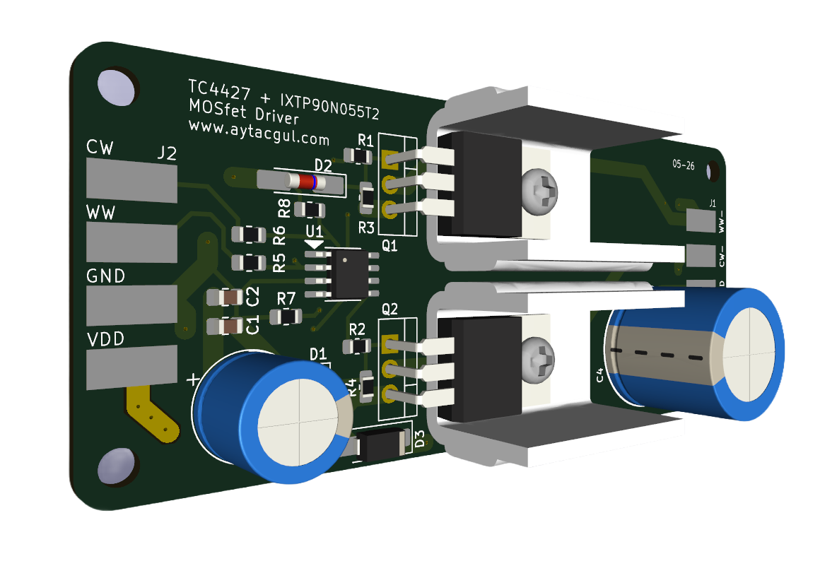
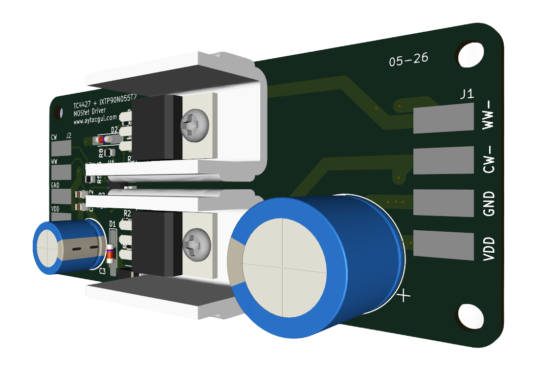
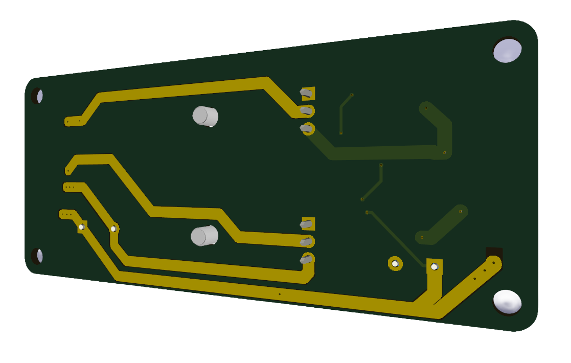
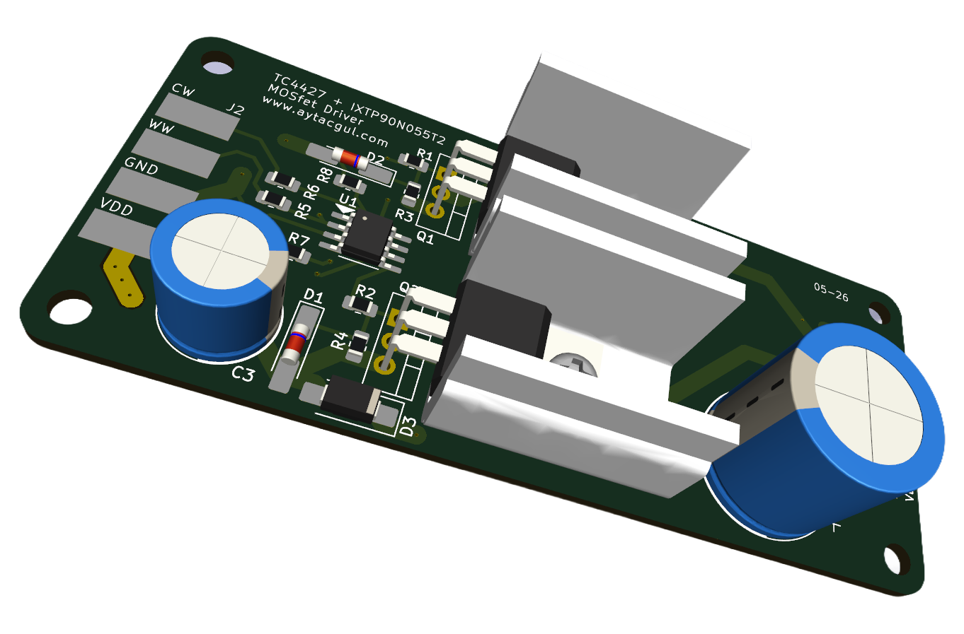
The PCB was designed in KiCad and is intentionally simple. The control electronics are located near the center of the board while the high-current MOSFETs and load connections are arranged around the outside.
The high-current paths use substantially wider copper than the signal traces. This is important because the voltage drop and heating of a PCB trace increase rapidly as load current increases.
The MOSFET gates, TC4427A outputs and associated gate components are also kept physically close together. Keeping the gate loop short reduces parasitic inductance and helps prevent ringing during fast switching transitions.
Four mounting holes allow the completed module to be mechanically secured inside an enclosure or lighting system.
Heatsinks
Each IXTP90N055T2 is fitted with an individual heatsink.
MOSFET conduction loss can be approximated by:
P = I² × RDS(on)
This means that doubling the load current results in approximately four times the conduction loss, assuming the MOSFET resistance remains constant.
In practice RDS(on) also increases as junction temperature rises, so thermal design becomes increasingly important at high current.
The large heatsinks used on this board therefore provide useful thermal headroom, especially when the circuit is installed in an enclosure or operated at high duty cycles.
PWM Operation
PWM dimming controls the average LED power by rapidly switching the MOSFET between fully on and fully off.
For example:
| PWM Duty Cycle | Approximate Output |
|---|---|
| 0% | Off |
| 10% | Very low brightness |
| 25% | Low brightness |
| 50% | Approximately half average power |
| 75% | High brightness |
| 100% | Continuously on |
The relationship between PWM duty cycle and perceived brightness is not perfectly linear because the human eye has a nonlinear response to light. A firmware gamma curve can be added when visually linear brightness adjustment is required.
PWM Frequency
For ordinary lighting applications I generally prefer a PWM frequency high enough to avoid visible flicker while remaining low enough that switching losses are insignificant.
Several hundred hertz to a few kilohertz is suitable for many LED applications. Higher frequencies are also possible, and the TC4427A is considerably faster than required for normal LED dimming.
The optimum frequency depends on the LED load, controller, required dimming resolution, EMC considerations and whether the light will be used with cameras.
Typical Applications
- High-power LED strip dimming
- Cool White / Warm White tunable lighting
- COB LED control
- Architectural lighting
- Photography lighting
- Workshop lighting
- Microcontroller-controlled lighting
- Two-channel PWM power switching
- General low-voltage DC load control
Important Current Considerations
The MOSFET's headline current rating should not be interpreted as the current rating of the completed board.
The practical output current depends on many factors:
- MOSFET junction temperature
- Heatsink thermal resistance
- Ambient temperature
- PCB copper thickness
- Trace width
- Solder joint quality
- Power cable cross-section
- Connector resistance
- PWM duty cycle
- PWM frequency
- Available airflow
For high-current operation the MOSFET temperature, PCB temperature and wiring should therefore be checked under the actual expected load rather than selecting the allowable current only from the MOSFET datasheet.
The finished board provides two compact high-current PWM channels with a proper MOSFET gate-drive stage, gate protection, transient protection, supply decoupling and substantial heatsinking.
Using the TC4427A instead of directly connecting the power MOSFETs to a microcontroller makes the design much more suitable for fast PWM operation and large MOSFET gate capacitances.
Although I built the board primarily as a Cool White / Warm White LED driver, it is essentially a general-purpose dual-channel low-side MOSFET power switch and can be adapted to many other DC switching applications.